Discover W25Q128JVSIQ Memory Chip Options for Your Projects
The W25Q128JVSIQ memory chip stands out for its versatility and performance in various applications. Users can explore multiple options when selecting this chip for their projects. From different manufacturers to various package types and configurations, the choices available cater to diverse project needs. Understanding these options helps in making informed decisions that enhance project outcomes.
Key Takeaways
The W25Q128JVSIQ memory chip offers high-speed data transfer, low power use, and strong reliability, making it ideal for many electronic projects.
Users can choose from different manufacturers, package types, and configurations to best fit their project needs and space constraints.
Checking compatibility with your system’s voltage, communication protocols, and physical size helps avoid common integration problems.
This chip suits a wide range of uses, including firmware storage, data logging, and automotive or industrial applications.
Consider your project’s storage, speed, temperature range, and budget to select the right W25Q128JVSIQ model for optimal performance.
Overview of W25Q128JVSIQ
The W25Q128JVSIQ memory chip offers a range of features that make it a popular choice for various applications. Its design focuses on high performance, reliability, and versatility, which are essential for modern electronic devices.
Key Features
The W25Q128JVSIQ boasts several notable features that enhance its functionality:
Memory Capacity: This chip provides 128M-bit (16M-byte) SPI flash memory, organized into 65,536 pages of 256 bytes each.
SPI Interface Speeds: It supports clock frequencies up to 133MHz in standard mode, 266MHz in dual mode, and 532MHz in quad mode, allowing for data transfer rates of up to 66MB/s.
Flexible Memory Erasure: Users can choose from various erase options, including 4KB sectors, 32KB and 64KB blocks, or a full chip erase.
Reliability: The chip offers an endurance of up to 100,000 program-erase cycles and ensures data retention for 20 years.
Continuous Read Feature: This feature supports wrap lengths of 8, 16, 32, and 64 bytes, which helps reduce latency during data access.
Power Efficiency: Operating at a voltage range of 2.7V to 3.6V, the chip consumes ultra-low power during standby (<1µA), making it suitable for battery-powered devices.
Operating Temperature Range: It functions effectively in harsh environments, with a temperature range of -40°C to +105°C.
Security Features: The chip includes write protection, power supply lockdown, One-Time Programmable (OTP) memory, block protection, and a unique 64-bit ID for authentication.
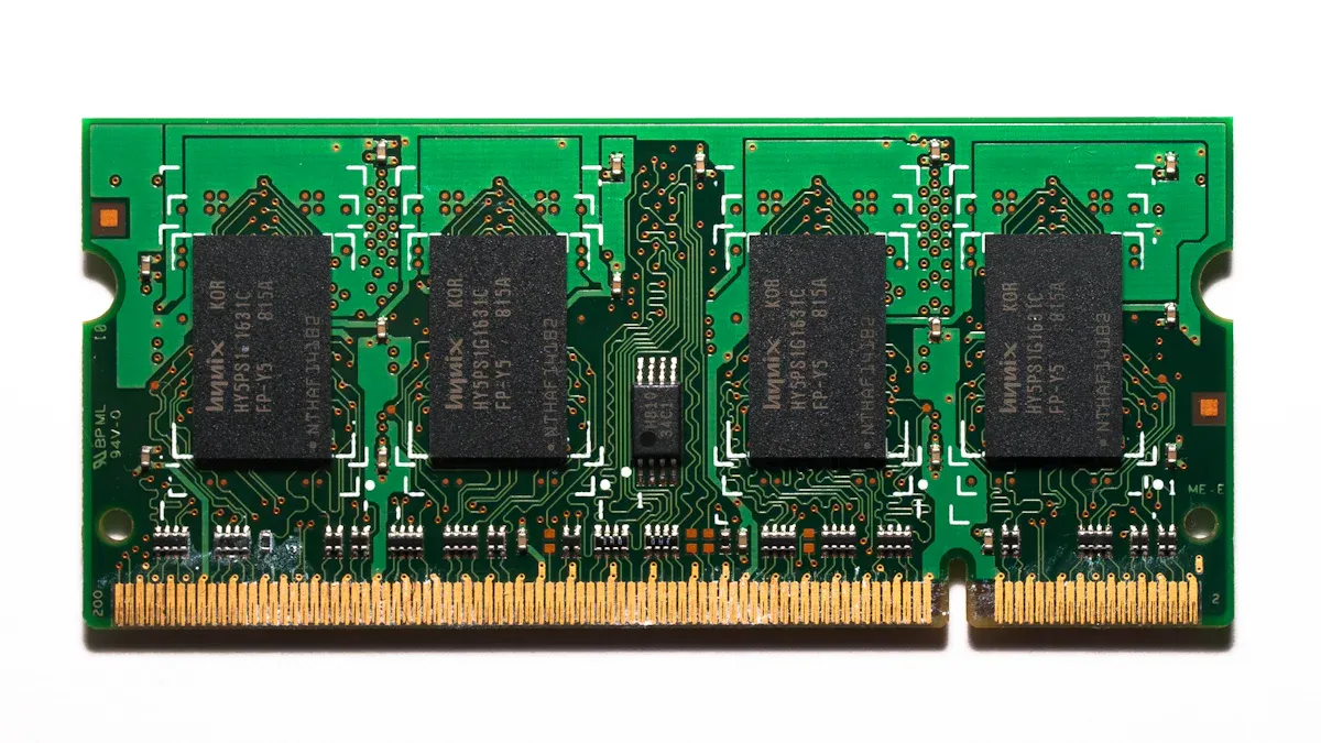
Compact Packaging: Available in options like the 8-pin SOIC and 24-ball WLCSP, it fits well in space-constrained designs.
These features collectively position the W25Q128JVSIQ as a high-performance memory solution, ideal for applications in consumer electronics, automotive systems, industrial controls, and IoT devices.
Technical Specs
The technical specifications of the W25Q128JVSIQ further highlight its capabilities. Below is a summary of its key specifications:
Specification | Details |
|---|---|
Storage Capacity | 128M-bit (16M-byte) Serial Flash Memory |
Voltage Range | 2.7V to 3.6V |
SPI Clock Frequency | Up to 133MHz (Standard SPI) |
Dual I/O Speed | Equivalent 266MHz (133MHz x 2) |
Quad I/O Speed | Equivalent 532MHz (133MHz x 4) |
Memory Organization | 65,536 pages of 256 bytes each |
Erase Sectors | 4KB sectors, 32KB and 64KB blocks |
Power Consumption | Ultra-low power-down current (<1µA) |
Operating Temp. | -40°C to +105°C |
The W25Q128JVSIQ's specifications demonstrate its suitability for a wide range of applications, particularly in embedded systems and consumer electronics. Its high-speed performance, combined with robust reliability and security features, makes it a preferred choice among engineers and developers.
W25Q128JVSIQ Options
Manufacturers
Several manufacturers produce the W25Q128JVSIQ memory chip, each offering unique features and support. Key players in the market include Winbond, Micron, and Cypress. These companies provide various options that cater to different project requirements. For instance, Winbond is known for its robust customer support and extensive documentation, which can be beneficial for developers during integration. Micron focuses on high-performance solutions, while Cypress emphasizes compatibility with a wide range of applications.
Package Types
The W25Q128JVSIQ memory chip is primarily available in an 8-pin SOIC package. This surface-mount form factor measures approximately 5.23mm by 7.9mm with a 1.27mm pin pitch. The compact design supports high-frequency operation up to 133 MHz and complies with RoHS standards, making it suitable for modern electronics. The precise footprint and symbol representations provided facilitate accurate schematic design and PCB layout. This compact SOIC-8 package enables efficient use of PCB space and compatibility with surface mount technology assembly, which is especially beneficial for space-constrained projects such as consumer electronics and portable devices.
Configurations
Manufacturers offer various configurations for the W25Q128JVSIQ memory chip. Below is a summary of the most common configurations:
Feature | Description |
|---|---|
Memory Organization | |
Sector Size | 4KB |
Operating Voltage | 2.7V to 3.6V |
SPI Interface | Standard SPI, Dual/Quad I/O SPI |
SPI Clock Frequency | Up to 133MHz |
Fast Read Speeds | 266MHz (Dual I/O), 532MHz (Quad I/O) |
Programmable Pages | 65536 pages of 256 bytes each |
Erase Granularity | 4KB sector erase, 32KB block erase, 64KB block erase, chip erase |
Package Type | SOIC-8, surface mount technology |
Power Consumption | As low as 1µA in standby mode |
Different configurations impact the chip's performance and integration into projects. For example, while the W25Q128JVSIQ and other chips in the series may have similar electrical specifications, variations in package types can lead to differences in system behavior. A user reported reboot failures when switching from an 8-SOIC package to an 8-WSON package, despite pin-to-pin compatibility. This highlights the importance of selecting the right package type for specific applications.
Compatibility with W25Q128JVSIQ
Determining Compatibility
When integrating the W25Q128JVSIQ memory chip into projects, several criteria help ensure compatibility with microcontrollers and other hardware. Consider the following factors:
Voltage Levels: Ensure that the voltage levels of the W25Q128JVSIQ match those of the microcontroller and other hardware.
Communication Protocols: Verify that the communication protocols are compatible to enable proper data exchange.
Signal Types: Confirm that signal types align to avoid system failures.
Physical Package Size: Check the physical package size and pin layout to fit existing design constraints.
Power Requirements: Consider power requirements to ensure the system can supply adequate power.
Operation Speed: Evaluate operation speed to meet performance needs.
Environmental Conditions: Account for environmental conditions to guarantee reliable operation.
These criteria collectively ensure smooth integration and optimal performance of the W25Q128JVSIQ memory chip within electronic systems.
Common Issues
Despite careful planning, users may encounter compatibility issues when using the W25Q128JVSIQ. One common problem arises from mismatched voltage levels, which can lead to device malfunction. Additionally, incorrect communication protocols may hinder data transfer, resulting in system errors.
Firmware updates and software support also play a crucial role in usability. They provide advanced programming capabilities, such as page, block, and sector programming modes, allowing precise and efficient firmware updates. The Winbond 25Q128JVSQ programmer supports multiple operating systems, making firmware updating accessible to a wide range of users. Its user-friendly interface simplifies complex programming tasks, even for beginners. Robust customer support ensures users can resolve issues and optimize chip usage. These features collectively maintain device performance, fix bugs, and enhance functionality, significantly improving the practical usability of the W25Q128JVSIQ memory chip.
Applications of W25Q128JVSIQ
The W25Q128JVSIQ memory chip finds extensive use across various applications due to its impressive features and capabilities. Its high-speed data transfer, low power consumption, and compact design make it suitable for numerous consumer electronics and industrial applications.
Use Cases
Common use cases for the W25Q128JVSIQ memory chip include:
Firmware Storage: The chip serves as reliable firmware storage in embedded systems, ensuring that devices operate smoothly.
Data Logging: It plays a crucial role in data logging for IoT devices, capturing essential information for analysis and monitoring.
Boot Memory: Many microcontrollers utilize the W25Q128JVSIQ as boot memory, allowing for quick startup and efficient operation.
Configuration Data Storage: The chip stores configuration data in consumer electronics, enabling users to customize device settings easily.
Industrial Control Systems: Its non-volatile memory capabilities make it ideal for industrial control systems that require consistent performance and data integrity.
The W25Q128JVSIQ's architecture supports efficient data management, making it a preferred choice for applications that demand frequent updates or precise data partitioning. Its reliability, with up to 100,000 program-erase cycles and 20 years of data retention, further enhances its appeal in consumer electronics.
Industry Applications
The W25Q128JVSIQ memory chip also plays a significant role in various industries, including automotive, industrial, and medical sectors. Below is a summary of its applications across these fields:
Application Area | Examples and Relevance |
|---|---|
Advanced Driver Assistance Systems (ADAS), automotive dashboards | |
Industrial Electronics | Automation systems, medical devices, safety equipment, programmable logic controllers |
Communication | Network devices, routers, and wireless access points supporting industrial communication needs |
Memory Features | 128M-bit capacity organized in 256-byte pages, flexible erase sizes (4KB sectors to full chip erase) |
SPI Interface | Standard, Dual, and Quad SPI with clock frequencies up to 133MHz, enabling fast data transfer |
Power Supply | Single 2.7V to 3.6V supply, low power consumption (as low as 1µA in power-down) |
Data Integrity and Security | JEDEC standard IDs, 64-bit unique serial number, security registers for data protection |
These features collectively enable the W25Q128JVSIQ to serve as a reliable, high-performance non-volatile memory solution in demanding applications. Its combination of high-speed SPI, flexible memory organization, low power consumption, and robust security features make it well-suited for embedded systems requiring reliable non-volatile storage.
Selecting the Right W25Q128JVSIQ
Choosing the right W25Q128JVSIQ memory chip for a project involves careful consideration of several factors. Understanding project requirements, performance benchmarks, and budget constraints can significantly influence the decision-making process.
Project Requirements
When selecting a memory chip, project requirements play a crucial role. Key factors to consider include:
Factor | Description / Consideration |
|---|---|
The W25Q128JVSIQ offers 128Mb of non-volatile serial flash memory, suitable for embedded systems and IoT devices. | |
Interface | Its SPI/QSPI compatible interface ensures broad compatibility with microcontrollers, facilitating ease of integration. |
Operating Voltage | The chip supports a wide voltage range (2.7V–3.6V), accommodating diverse power needs. |
Package Type | Available in 8-pin DIP and surface-mount designs, the chip simplifies PCB integration and automated assembly. |
Read Speed | Models vary in read speed: Base (50MB/s), Advanced (65MB/s), Pro (80MB/s), allowing selection based on speed needs. |
Operating Temperature | The chip operates effectively in temperatures ranging from -40°C to +85°C, with some models extending to -40°C to +105°C for harsh environments. |
Data Integrity | Built-in ECC technology ensures reliable data storage in high-interference or critical applications. |
Environmental Compliance | RoHS compliance ensures suitability for eco-conscious and regulatory-compliant projects. |
Model Selection | Choose the Base model for general use, the Advanced model for faster data access in industrial applications, and the Pro model for extreme environments. |
These considerations help tailor the W25Q128JVSIQ chip variant to specific project needs.
Performance Considerations
Performance benchmarks are vital when evaluating the W25Q128JVSIQ. The chip's specifications demonstrate its capabilities in real-world applications:
Feature | Specification/Benchmark |
|---|---|
Read Speed (Standard SPI) | Up to 104 MHz |
Read Speed (SPI Clock) | Up to 133 MHz |
Read Speed (Dual SPI) | Up to 266 MHz |
Read Speed (Quad SPI) | Up to 532 MHz |
Data Transfer Rate | Up to 66 MB/s |
Write Speed | Up to 16 MHz |
Endurance | 100,000 program-erase cycles |
Data Retention | 20 years |
Operating Voltage Range | 2.7 V to 3.6 V |
Power Consumption | Ultra-low power-down current < 1 µA |
Operating Temperature Range | -40°C to +105°C |
Package Options | 8-pin SOIC, 24-ball WLCSP |
Special Features | Continuous Read, erase/program suspend, security options (write-protect, OTP, block protection), unique 64-bit ID |
These benchmarks illustrate the W25Q128JVSIQ's suitability for demanding applications, where fast data access, reliability, and low power consumption are critical.
Budget Constraints
Budget constraints also influence the selection process. The W25Q128JVSIQ memory chip offers competitive pricing, making it accessible for various projects. For instance, the unit price ranges from approximately $0.51 for single units to about $0.31 when purchased in bulk (1000 units). This pricing structure allows developers to choose options that fit their financial plans while ensuring they do not compromise on quality or performance.
In summary, the W25Q128JVSIQ memory chip offers a versatile solution for various projects. Users can benefit from its multiple features, including flexible data management and low power consumption. Here are some recommendations for those considering this chip:
The W25Q128JVSIQ supports Standard, Dual, and Quad SPI communication modes, allowing users to balance speed and complexity based on project requirements.
It comes in an 8-pin SOIC package, suitable for designs with limited board space.
Software reset mechanisms improve system stability and enable autonomous recovery from errors.
Users should verify the footprint accuracy against datasheets to avoid PCB design issues and costly revisions.
Exploring these options can lead to enhanced performance and reliability in your projects.
FAQ
What is the W25Q128JVSIQ memory chip used for?
The W25Q128JVSIQ memory chip is commonly used for firmware storage, data logging, and boot memory in embedded systems and IoT devices.
How does the W25Q128JVSIQ compare to other memory chips?
The W25Q128JVSIQ offers high-speed data transfer, low power consumption, and a compact design, making it suitable for various applications compared to other memory chips.
What are the power requirements for the W25Q128JVSIQ?
The W25Q128JVSIQ operates within a voltage range of 2.7V to 3.6V, ensuring compatibility with many microcontrollers and electronic systems.
Can the W25Q128JVSIQ be used in automotive applications?
Yes, the W25Q128JVSIQ is suitable for automotive applications, including advanced driver assistance systems and automotive dashboards, due to its reliability and performance.
What packaging options are available for the W25Q128JVSIQ?
The W25Q128JVSIQ is primarily available in an 8-pin SOIC package, which is ideal for space-constrained designs and surface mount technology.
See Also
Breakthroughs Fueling Homegrown Memory Chip Production In 2025
Best USB To Serial Interface IC Chips For 2025 Projects
Leading Microcontrollers Powering Embedded Systems In 2025
Evaluating Similar Microchips Used For Pet Identification
Current Developments Influencing The Analog IC Market In 2025