What Are Photonic Integrated Circuits and How Do They Work
Photonic integrated circuits, also called planar lightwave circuits or integrated optical circuits, combine many optical components on a single chip. These circuits use photons instead of electrons to process and carry information. Scientists often build them using semiconductor materials like silicon or indium phosphide. Photonic integrated circuits can generate, move, change, and measure light. By mounting different optical devices together, they make technology smaller, more stable, and more efficient.
Key Takeaways
Photonic integrated circuits use light to process and carry information, making devices faster and more energy efficient.
These circuits combine key parts like lasers, modulators, detectors, and waveguides on a single chip to control light precisely.
Compared to electronic circuits, photonic circuits offer higher speed, larger bandwidth, lower power use, and less heat.
They play a vital role in telecommunications, data centers, and healthcare by enabling faster data transfer and better sensing.
Designing and making photonic chips involves careful material choice, precise layout, and advanced manufacturing to ensure performance and reliability.
Components

Key Elements
Photonic chips contain several important parts that work together to control light. Each part has a special job:
Lasers: Create the light needed for the circuit.
Modulators: Change the light to carry information.
Detectors: Read the light and turn it into electrical signals.
Waveguides: Guide the light along paths on the chip.
Splitters: Divide the light into different paths.
Combiners: Bring light from different paths together.
Amplifiers: Make the light signal stronger.
These elements allow signals to move at the speed of light. They help send data quickly and with little energy loss. By putting all these parts on one chip, engineers can make devices that are small, fast, and use less power. This makes them useful in phones, computers, and sensors.
Materials
Scientists use different materials to build these chips. Each material has its own strengths and weaknesses. The table below shows some common materials and their properties:
Material | Key Properties and Uses | Limitations and Challenges |
|---|---|---|
Indium Phosphide (InP) | Direct bandgap, good for making and detecting light, works well for lasers and detectors, used in communication | Hard to make, costs more, needs special factories |
Silicon (Si) and Silicon Dioxide (SiO2) | Cheap, easy to make, works well for guiding light, used with electronics | Cannot make light easily, cannot detect some light colors, limited for some uses |
Gallium Arsenide (GaAs) | Good for short light waves, used in sensors and special lasers | Not used much for communication, costs more, harder to make |
Lithium Niobate (LiNbO3) | Great for changing light quickly, used in modulators | Cannot make or detect light, hard to use for big chips |
New materials like graphene and metamaterials are also being studied. These can make chips even smaller and faster. Better ways to build chips, like using special light to make tiny parts, help improve performance. Some researchers mix different materials on one chip to get the best features from each.
Operation
How Photonic Integrated Circuits Work
Photonic integrated circuits use light to move and process information on a chip. These circuits work by guiding photons through tiny paths called waveguides. Each part of the circuit, such as lasers, modulators, and detectors, has a special job in handling the light.
Lasers create the light that starts the process.
Waveguides carry the light to different parts of the chip.
Modulators change the light so it can carry data.
Detectors read the light and turn it into electrical signals.
Photonic integrated circuits use a laser source to inject light, much like electronic circuits use electrical current. The light travels through the chip, passing through each component to process and distribute information. This method allows the chip to handle large amounts of data quickly and with less energy. By putting all these parts on one chip, engineers can make devices smaller, faster, and cooler than traditional electronics.
Note: Photonic integrated circuits can perform many optical functions on a single chip. This includes generating, moving, changing, and measuring light. The integration of these parts leads to higher bandwidth, lower power use, and less heat.
Light Manipulation
Photonic integrated circuits control light in many ways to send and receive information. They use special components to guide, split, and switch light paths.
Waveguides act as tiny roads for light, keeping it on track inside the chip.
Optical couplers and beam splitters divide light into different paths or combine it from several sources.
Optical switches direct light between different waveguides, allowing the circuit to change routes as needed.
Multiplexing lets several signals travel together in one waveguide, making the system more efficient.
Some circuits use nano-antennas to change the way light moves inside the waveguide. Programmable interferometric meshes, like Mach-Zehnder interferometers, help control the strength and phase of light. This allows the chip to create special light patterns or separate different types of light signals.
Photonic integrated circuits also use optical isolators to protect lasers. These isolators let light pass in only one direction, which keeps the laser safe and stable. New designs, such as non-magnetic isolators, work well with silicon chips and help make the circuits more flexible.
Unlike traditional optical systems that use large lenses and mirrors, photonic integrated circuits use tiny waveguides and other small parts. This design keeps energy loss low and makes the circuits more compact. The chip can handle complex tasks like changing the color of light or boosting its strength, all in a small space. This makes photonic integrated circuits ideal for fast communication, sensing, and new technologies that need speed and efficiency.
Photonic Integrated Circuits vs. Electronic Circuits

Differences
Electronic circuits and photonic integrated circuits process information in very different ways. Electronic circuits use electrons that move through wires and other components. These electrons interact with other particles, which slows them down and causes heat. Photonic integrated circuits use photons, or particles of light, to carry signals. Photons travel at the speed of light and do not interact much with other particles, so they move faster and lose less energy.
The table below shows some key differences:
Characteristic | Electronic Circuits | Photonic Integrated Circuits (PICs) |
|---|---|---|
Signal Carrier | Electrons (electrical signals) | Photons (light signals) |
Speed | Limited by electron drift speed | Near speed of light |
Bandwidth | Lower bandwidth | Higher bandwidth |
Power Consumption | Higher due to energy loss and heat | Lower due to minimal energy loss |
Interference Immunity | Susceptible to electromagnetic interference | Immune to electromagnetic interference |
Components Used | Transistors, resistors, capacitors | Waveguides, lasers, modulators, detectors |
Photonic integrated circuits use waveguides to guide light, while electronic circuits use wires to guide electrons. Modulators in photonic circuits change the light’s properties, such as its phase or frequency, to encode data. In electronic circuits, voltage or current changes carry information. Photonic circuits also use photodetectors to turn light into electrical signals when needed.
Advantages
Photonic integrated circuits offer several important advantages over electronic circuits:
They can send data much faster because photons move at the speed of light.
They support much higher bandwidth, so they can carry more information at once.
They use less power and produce less heat, making them more energy efficient.
They do not suffer from electromagnetic interference, which makes them safer and more reliable.
They allow for multiplexing, which means many signals can travel together in one waveguide.
Their small size helps make devices more compact.
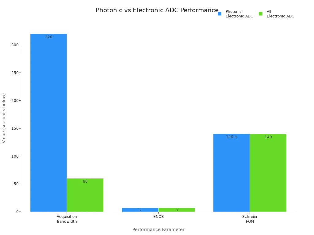
The chart below shows how photonic circuits can achieve much higher bandwidth than electronic circuits:
Photonic integrated circuits help solve problems like heat and limited speed in electronics. They are now used in fields that need fast, reliable data transfer, such as telecommunications and data centers.
Applications
Photonic integrated circuits have changed many industries by making technology faster and more efficient. These chips now play a key role in telecommunications, data centers, and healthcare.
Telecommunications
Telecommunications companies use photonic integrated circuits to send large amounts of data quickly and safely. These chips help build fast internet connections and support new networks like 5G and IoT. The table below shows how these circuits work in different parts of telecom systems:
Application Area | Common PIC Components and Uses | Advantages in Telecommunications |
|---|---|---|
Optical Communications | Transceivers, amplifiers, multiplexers, wavelength demultiplexers | Higher speed, bandwidth, power efficiency |
Integrated Transmitter Circuits | Monolithic integrated transmitter laser circuits | Compact size, low transmission loss |
Receivers | Integrated tunable receivers | Enhanced reliability, improved optical alignment |
Lasers and Modulators | Distributed feedback lasers and modulators | Increased bandwidth, low-loss couplers |
Repeaters | Monolithic integrated repeater chips | Mass production, reduced costs |
Wavelength Demultiplexers | Monolithic integrated optical wavelength demultiplexers | Immune to electromagnetic interference |
Microwave Photonics | High-frequency signal processing, beamforming in 5G and satellite | Wide bandwidth, secure from monitoring, low power consumption |
Photonic integrated circuits allow telecom networks to move data at speeds up to 800 Gbps. They also lower power use and make networks more flexible.
Data Centers
Data centers rely on photonic integrated circuits to handle huge amounts of information. These chips help connect servers and storage devices with light, not electricity. This change makes data centers faster and cooler. Some benefits include:
Data moves at the speed of light, reducing delays.
Power use drops by up to 60%, saving money and energy.
Less heat means less need for cooling systems.
Data centers can handle up to 500% more traffic without using more power.
Silicon photonics is common in these centers. Companies use millions of these chips each year to keep up with cloud computing and AI needs.
Sensing and Healthcare
Healthcare and sensing use photonic integrated circuits for better testing and monitoring. Doctors use these chips in small devices to check for diseases or track health signs. Some uses include:
Portable tools for early disease detection, like cancer or eye problems.
Wearable devices that measure heart rate, oxygen, and blood sugar.
Sensors that find tiny amounts of gases or toxins in the air.
Fast blood tests at home or in clinics.
Application Area | Measurable Benefits and Metrics | Additional Qualitative Benefits |
|---|---|---|
Medical Diagnostics | Detects proteins at very low levels, real-time results, works in small devices | High sensitivity, low cost, easy to use anywhere |
Environmental Sensing | Finds heavy metals and gases at low amounts, real-time monitoring | Selective detection, portable, works in remote places |
These advances help doctors diagnose diseases sooner and keep people healthier. They also help protect the environment by finding pollution quickly.
Design and Fabrication
Design Process
Designers follow a clear set of steps to create a photonic chip. Each step helps ensure the chip meets its goals for size, cost, and performance.
Define the main reasons for making the chip and set system requirements, such as how small or complex it should be.
Select the right material and platform, like silicon or indium phosphide, based on what the chip needs to do.
Break down the system into smaller parts and choose the best building blocks for each function.
Use Process Design Kits (PDKs) to design, simulate, and test each part. PDKs give access to trusted building blocks, such as waveguides and modulators, and help protect the foundry’s special designs.
Lay out the circuit, making sure waveguides and electrical contacts fit well and follow the rules for making chips.
Move to fabrication, then test, package, and check the finished chip.
Designers use special software to help with each step. Popular tools include Cadence, Silvaco, and Synopsys RSoft. These programs let engineers draw circuits, run simulations, and check for errors. They also help combine electronic and photonic parts on the same chip.
Engineers must check for errors in the design, like making sure parts are not too close together. They also follow rules to make the chip easier to build and more reliable. Hybrid designs, which use more than one material, need extra care to match materials and keep the chip stable.
Manufacturing
Most photonic chips are made using silicon photonics and CMOS-compatible foundry processes. This method uses the same technology as computer chips, which allows for high-volume production and small features. Foundries like AIM Photonics offer Multi-Project Wafer (MPW) runs, letting many designers share a single wafer to lower costs.
Manufacturing steps include layout, verification, fabrication, packaging, and testing. The process uses advanced tools to etch and deposit materials with high accuracy. However, making these chips at scale brings challenges:
Keeping device yields high and coupling efficiency stable.
Managing heat and matching materials in hybrid chips.
Avoiding defects from tiny imperfections.
Aligning different materials with great precision.
Recent breakthroughs include new pilot production lines in China and advances by Intel Labs. These efforts focus on faster, smaller, and more energy-efficient chips. New materials like lithium tantalate also help make chips with lower loss and higher speed, opening the door to better sensors and faster data links.
Photonic integrated circuits use light to process and move information. They offer high speed, large bandwidth, and low power use. These circuits now help drive fast data centers, 5G networks, and new medical tools. Experts expect the market to grow quickly, reaching over $22 billion by 2034. The table below shows how their speed and efficiency compare to regular chips.
Characteristic | Conventional Integrated Circuits | Photonic Integrated Circuits |
|---|---|---|
Speed | Low | High |
Bandwidth | Low | High |
Power Efficiency | Low | High |

These advances will shape the future of technology in many industries.
FAQ
What is the main use of photonic integrated circuits?
Photonic integrated circuits help move and process data using light. Many companies use them in fast internet, data centers, and medical devices. These chips make technology faster and more energy efficient.
How do photonic integrated circuits save energy?
Photonic integrated circuits use light instead of electricity to send signals. Light loses less energy as it travels. This means devices with these chips use less power and produce less heat.
Can photonic integrated circuits replace electronic circuits?
Engineers use photonic integrated circuits for tasks that need high speed and large bandwidth. Electronic circuits still work better for some jobs. Many devices now use both types together.
What materials do engineers use to make photonic integrated circuits?
Engineers often use silicon, indium phosphide, gallium arsenide, and lithium niobate. Each material has special strengths. Some work better for guiding light, while others help create or detect light.
Are photonic integrated circuits safe to use?
Yes, photonic integrated circuits are safe. They do not create harmful electromagnetic interference. Devices with these chips often run cooler and more reliably than older electronic devices.
See Also
Understanding Optocoupler IC Chips And Their Operation
Exploring The Roles And Applications Of Photodiode Sensors
A Comprehensive Guide To Fully Integrated Processor Functions