What Are Photonic Circuits and How Do They Work

Photonic circuits are integrated structures that process and transmit light signals on flat chips. They use photons, or particles of light, instead of electrons to carry information. This design allows devices like modulators and detectors to work together efficiently on a single chip. Many industries use photonic circuits because they enable faster data transmission, lower energy use, and support advanced technologies such as high-speed internet, data centers, and autonomous vehicles.
Key Takeaways
Photonic circuits use light instead of electricity to send and process data, making them faster and more energy-efficient than traditional electronic circuits.
These circuits guide light through tiny paths called waveguides and use components like lasers, modulators, and detectors to control and detect light signals.
Photonic circuits offer huge benefits such as faster data speeds, lower power use, less heat, and support for advanced technologies like high-speed internet and quantum computing.
Challenges include complex manufacturing, material integration, and the need for skilled engineers, but ongoing innovations are making photonic circuits more reliable and affordable.
Photonic circuits are widely used in data centers, telecommunications, autonomous vehicles, and medical sensing, with a growing market expected to reach billions in value soon.
Photonic Circuits Basics

What They Are
Photonic circuits are tiny chips that use light to carry and process information. These circuits use special parts that guide, control, and detect light. Unlike electronic circuits, which use electricity and electronic parts like transistors and resistors, photonic circuits use optical parts such as waveguides, lasers, and detectors. This change from electrons to photons helps solve problems like heat buildup and slow data speeds.
Note: Photonic circuits can move data much faster and use less energy than traditional electronic circuits.
The table below shows the main differences between electronic and photonic circuits:
Aspect | Electronic Integrated Circuits (EICs) | Photonic Integrated Circuits (PICs) |
|---|---|---|
Signal Type | Electrical signals (electrons) | Light signals (photons) |
Components | Transistors, resistors, capacitors, diodes | Waveguides, lasers, modulators, detectors |
Signal Manipulation | Electrical currents | Light using optical components |
Advantages | Foundation of electronics | High bandwidth, low power, fast transmission |
Operating Principle | Electron flow in semiconductors | Light guided by optical components |
Applications | Phones, computers, gadgets | Optical communication, sensing, computing |
Limitations Addressed | Heat, density limits | Overcomes heat and density issues |
Photonic circuits come in different types. Some only guide light (passive), while others can create, change, or detect light (active). Engineers also group them by size, from small chips with a few parts to large chips with many functions. The material used to make these circuits can be silicon, indium phosphide, or other special materials.
How They Work
Photonic circuits work by moving photons through tiny paths called waveguides. These waveguides act like roads for light, keeping it on track as it travels across the chip. Lasers or other light sources send photons into the circuit. Modulators change the light’s properties, such as its brightness or phase, to carry information. Detectors at the end of the circuit sense the light and turn it back into electrical signals if needed.
Photonic circuits use several tricks to control light:
They adjust the phase or timing of light with phase shifters.
They use modulators to encode data onto the light.
They detect light with special sensors.
Some advanced photonic circuits can even handle quantum information. They do this by changing properties like polarization or path, and by using special devices to perform logic operations with photons. These circuits can combine many optical parts on one chip, making them compact and stable.
💡 Photonic circuits can process information at the speed of light, making them ideal for high-speed internet, data centers, and even quantum computers.
Components
Waveguides
Waveguides act as the highways for light in photonic circuits. They keep photons moving in the right direction across the chip. Engineers use materials with a higher refractive index for the core and a lower index for the cladding. Silicon often serves as the core, while quartz or silica forms the cladding. This design traps light inside the waveguide. Multi-micron waveguides offer low phase error, better thermal management, and easy integration with lasers and detectors. These waveguides also match well with optical fibers, making connections simple and efficient.
Waveguide Structure | Advantages |
|---|---|
High light confinement, low loss, flexible design | |
Strip-loaded Waveguides | Efficient coupling of light |
SOI Waveguides | Popular for integration, compatible with standard fabrication |
Other types include rib, segmented, and photonic crystal waveguides. Each type offers unique benefits, such as strong light control or 3D integration.
Light Sources
Light sources generate the photons that travel through the circuit. The most common sources are lasers, especially those made from III–V semiconductors. These lasers provide high efficiency, strong output power, and work well in different temperatures. Silicon-based lasers exist, but they face challenges with efficiency. Engineers often combine III–V lasers with silicon chips to get the best performance. Some circuits use external lasers, while others use on-chip sources.
Light Source Type | External Laser Needed | Efficiency | Maximum Output Power | Notes on Performance and Integration |
|---|---|---|---|---|
III–V Semiconductor Lasers | No | Above 176 mW | High efficiency, high output power | |
Silicon-based Raman Lasers | Yes | Up to 28% | N/A | Lower efficiency, long cavity |
Heterogeneous III–V on Si Lasers | No | 12.7–37% | 1.8–185 mW | Combines advantages of both |
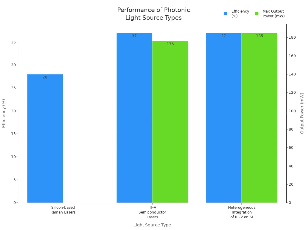
Lasers like DFB and VCSELs offer high stability, low power use, and fast data rates. Quantum Dot lasers add better temperature stability and longer lifetimes.
Modulators
Modulators encode information onto the light. They change the amplitude, phase, or polarization of photons as they pass through the waveguide. By applying an electric field, modulators adjust the refractive index of the material, which changes the light signal. Mach-Zehnder Interferometer (MZI) modulators and ring resonator modulators are the most common types. MZI modulators use phase shifts to control light, while ring resonators rely on resonance for compact size and low voltage operation. Modulators allow photonic circuits to send data at very high speeds.
Detectors
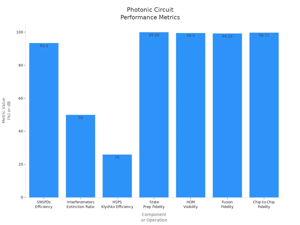
Detectors sense the light at the end of the circuit and convert it into electrical signals. They use effects like the photovoltaic and photoelectric effects to generate current when photons hit the detector. Photodiodes and avalanche photodiodes are common choices. These devices offer high quantum efficiency, with values around 72% at 400 nm and 79% at 600 nm. Fast response times and high sensitivity make them ideal for data communication.
Detection Mechanism | Principle | Typical Devices |
|---|---|---|
Photon ejects electron | Photomultiplier tubes | |
Photovoltaic Effect | Photon creates voltage/current | Photodiodes, solar cells |
Photoconductive Effect | Photon increases conductivity | Photoresistors |
Tip: The combination of waveguides, light sources, modulators, and detectors allows photonic circuits to guide, generate, encode, and detect light with high speed and accuracy.
Advantages and Challenges
Benefits
Photonic circuits offer several important advantages over traditional electronic circuits. They use photons, which move at the speed of light and do not face resistance like electrons. This allows photonic circuits to transmit multiple data streams at once with much less energy loss. As a result, data moves faster and with lower power consumption. Data centers that use photonic circuits can reach terabit speeds, switch in nanoseconds, and use about half the power of electronic systems. This leads to significant cost savings and supports the growing needs of cloud computing.
Recent research shows that photonic integrated circuits (PICs) can transmit data up to three times faster than electronic circuits. They also provide up to ten times better data transfer efficiency, one hundred times higher bandwidth, and about 70% lower latency. PICs generate less heat, which allows for higher routing density and better thermal management. These features make them ideal for high-speed imaging, national defense, and artificial intelligence.
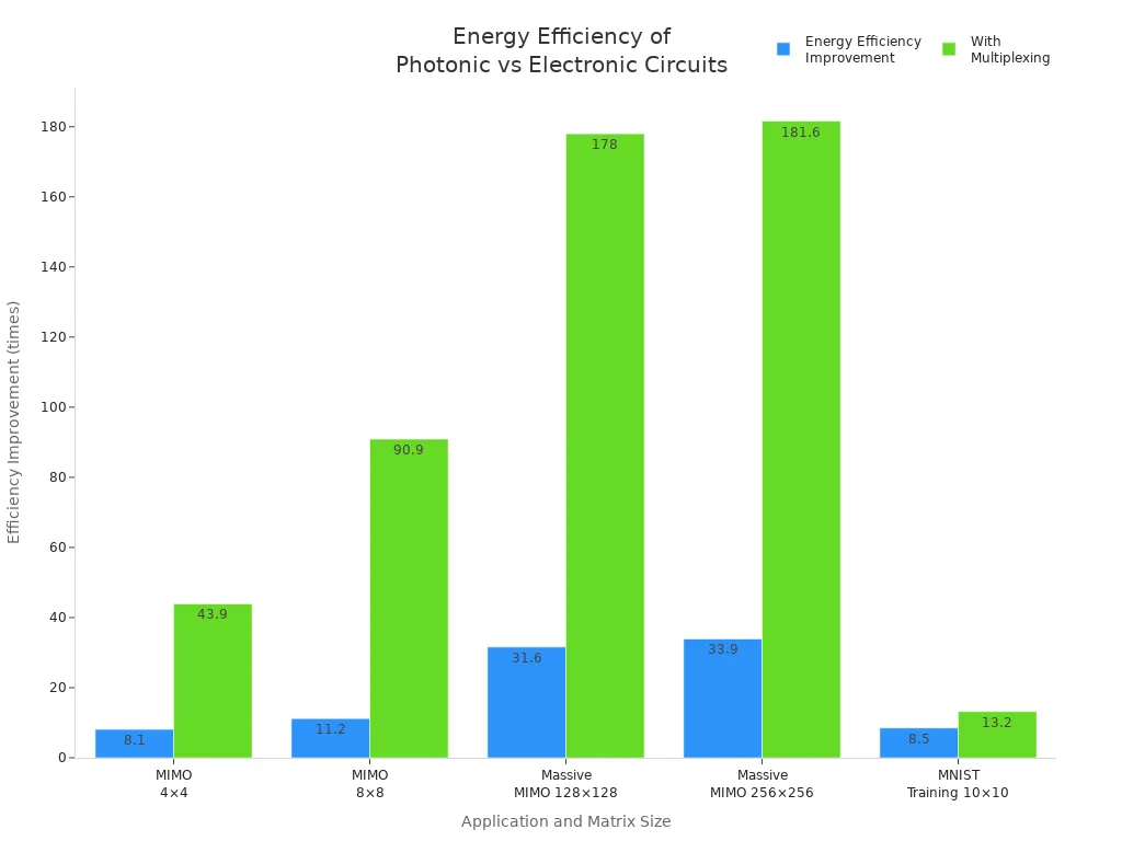
The table below compares the energy efficiency improvements of photonic circuits in real-world applications:
Application | Matrix Size (N×N) | Processing Time Saved (per day) | Energy Saved (per day) | Energy Efficiency Improvement (times) |
|---|---|---|---|---|
MIMO | 4×4 | 0.15 ms – 25 min | 27.3 µJ – 273 J | 8.1 (up to 43.9 with multiplexing) |
MIMO | 8×8 | 1.18 ms – 3.3 h | 211.8 µJ – 2.1 kJ | 11.2 (up to 90.9 with multiplexing) |
Massive MIMO | 128×128 | 0.53 s – 1472 h | 95.7 mJ – 957 kJ | 31.6 (up to 178 with multiplexing) |
Massive MIMO | 256×256 | 2.16 s – 6000 h | 0.39 J – 3.9 MJ | 33.9 (up to 181.6 with multiplexing) |
MNIST Training | 10×10 | 14.4 ms | 2.6 mJ | 8.5 (up to 13.2 with multiplexing) |
💡 Photonic circuits help reduce energy use and heat, making them a smart choice for future technology.
Limitations
Despite their many benefits, photonic circuits face several technical challenges:
Manufacturing photonic circuits requires high precision and complex processes, which increases costs.
Material limitations can affect performance and compatibility.
Integrating different materials, such as combining silicon and indium phosphide, remains difficult.
Active components like lasers and modulators may consume high power.
Devices can be sensitive to temperature changes, which may impact performance.
Testing and troubleshooting photonic circuits need special equipment and skills.
The diversity of photonic components is still limited compared to electronic parts.
Propagation loss can weaken light signals as they travel through waveguides.
Precise alignment and calibration are time-consuming and costly.
There is a shortage of skilled professionals in photonic engineering.
Scaling up production for mass use also presents obstacles. Silicon photonics depends on silicon-on-insulator wafers, but these cannot generate coherent light, so engineers must add indium phosphide lasers. The difference in wafer sizes and integration methods affects cost and production speed. Achieving high integration density and combining photonic and electronic functions on one chip remains a major challenge for the industry.
Photonic Circuits vs Electronic Circuits

Speed and Bandwidth
Photonic circuits move data using photons, which travel almost as fast as light. This speed is much greater than the speed of electrons in wires. As a result, photonic circuits can send information much faster than electronic circuits. They also support higher bandwidth, which means they can carry more data at once.
Photons do not create electromagnetic interference, so signals stay clear and stable.
Photonic circuits lose less energy as heat, making them more efficient.
Data centers and telecommunication systems use these circuits to handle huge amounts of data quickly.
In real-world tests, photonic circuits have processed signals like 6 GHz radar and 8 Gbit/s communication, which is beyond what most electronic circuits can do.
📈 Photonic circuits help companies achieve faster internet speeds and better performance in AI and cloud computing.
The ability to change the phase and polarization of light gives photonic circuits more ways to represent data. This feature increases their bandwidth even further. Microwave photonics can also turn radio signals into light, which boosts bandwidth and lowers delays.
Power and Size
Photonic circuits use less power because photons do not face resistance like electrons. This means less heat and lower energy bills. These circuits also allow for dense data routing, which is important for large data centers.
Electronic circuits are still smaller in many cases. Engineers have made electronic chips very tiny over many years. Photonic circuits are catching up, thanks to new imaging and manufacturing methods. For example, scientists now use advanced imaging to see how light moves inside a chip. This helps them design even smaller and better circuits.
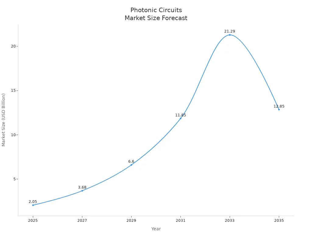
The market for photonic integrated circuits is growing fast. Companies use silicon and other materials to make these circuits smaller and more powerful. By 2030, experts expect the market to reach over $40 billion. As technology improves, photonic circuits will continue to shrink and become more common in everyday devices.
Applications and Materials
Key Uses
Photonic technology plays a central role in modern data centers and telecommunications. Companies use optical interconnects to replace copper wiring, which enables faster and more energy-efficient data transfer. Silicon photonic transceivers now support data rates of 100 gigabits per second and higher. These devices allow rapid data transmission over distances greater than 10 meters and help connect AI accelerators for better scalability. Optical switches improve data routing speed and network flexibility. The market for these devices is growing quickly, with new products reaching 800G and even 1.6T speeds. Beyond communications, engineers use photonic chips in LiDAR for autonomous vehicles, biosensing for medical diagnostics, and quantum computing. In quantum computing, photonic chips use quantum effects like superposition and entanglement to process information at high speed and with low noise.
Application Area | Example Uses |
|---|---|
Data Centers | High-speed transceivers, optical switches |
Telecommunications | Long-distance data transmission, WDM systems |
Quantum Computing | Qubit processing, entangled photon generation |
LiDAR | 3D sensing for vehicles and robotics |
Biosensing | Medical diagnostics, environmental monitoring |
Note: Photonic circuits help meet the growing needs of AI, cloud computing, and advanced sensing.
Materials
Engineers select materials based on the function and performance needed. Silicon is the most common choice because it works well with existing chip manufacturing and offers high refractive index contrast. Silicon-on-insulator (SOI) structures improve light confinement and reduce losses. III-V semiconductors like indium phosphide (InP) and gallium arsenide (GaAs) are used for lasers and detectors due to their efficient light emission. Other materials, such as lithium niobate, silicon nitride, and chalcogenide glasses, provide special properties for modulators and low-loss waveguides.
Material Type | Properties and Applications |
|---|---|
Silicon (Si) | High refractive index, CMOS compatible, ideal for waveguides |
Silicon-on-Insulator (SOI) | Enhanced light confinement, low loss |
III-V Semiconductors (InP, GaAs) | Efficient light emission, used in lasers and detectors |
Lithium Niobate (LiNbO3) | High electro-optic effect, used in modulators |
Silicon Nitride (Si3N4) | Low optical loss, used in high-Q resonators |
Polymers | Flexible, low-cost, tunable properties |
Silicon photonics allows integration with electronics on the same chip, reducing energy use and supporting miniaturization. However, silicon cannot emit light efficiently, so engineers often combine it with III-V materials for better performance.
Manufacturing
Manufacturing photonic devices requires high precision. Factories use advanced lithography and leverage mature CMOS processes to produce chips at scale. Challenges include integrating photonics and electronics, managing heat, and packaging. Laser integration remains difficult because silicon cannot emit light directly. To solve these issues, engineers use hybrid integration, multi-die packaging, and improved waveguide designs. Open-access foundries and better wafer quality also help lower costs and speed up innovation.
Tip: New solutions like microfluidic cooling and process design kits are making photonic manufacturing more reliable and scalable for future technologies.
Photonic technology continues to shape the future of data centers, AI, and quantum computing. Recent progress includes:
Integration of electronic and optical parts on one chip for efficient systems.
New materials like Thin Film Lithium Niobate and Barium Titanite that boost performance.
Co-packaged optics that improve network switches and AI networks.
Growth in programmable and software-defined photonics.
Aspect | Summary |
|---|---|
Market Growth | Experts predict the global market will reach nearly $98 billion by 2034. |
Key Applications | Data centers, 5G, quantum computing, LiDAR, and AI benefit the most. |
Technological Impact | Higher bandwidth, lower latency, and better energy efficiency. |
New trends and investments show that photonics will keep changing how people connect and compute. Staying updated on these advances helps everyone understand the future of technology.
FAQ
What is the main difference between photonic and electronic circuits?
Photonic circuits use light (photons) to carry information. Electronic circuits use electricity (electrons). Photonic circuits move data faster and use less energy.
Can photonic circuits replace all electronic circuits?
Photonic circuits work best for high-speed data and communication. They cannot replace all electronic circuits because some devices need electrical signals for power or control.
Are photonic circuits safe to use?
Photonic circuits do not emit harmful radiation. They use light at safe wavelengths. Engineers design these circuits to meet strict safety standards.
Where can people see photonic circuits in action?
Data centers
High-speed internet connections
LiDAR in self-driving cars
Quantum computers
These examples show how photonic circuits help modern technology.
See Also
Understanding Optocoupler IC Chips And Their Operation
Exploring The Functions And Applications Of Photodiode Sensors
How Optocouplers Function Within AC And DC Circuits
An Overview Of Fast Ethernet Transceiver ICs And Their Function