How the PCB Manufacturing Process Works from Design to Finished Board
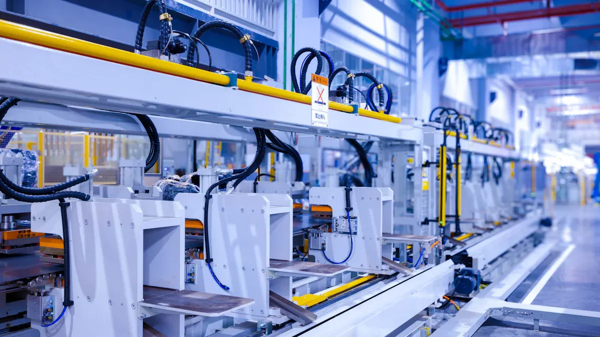
You turn your electronic design into a working product by following a series of clear steps in the pcb manufacturing process. You start with your circuit idea and move through design, material selection, and precise imaging. You then see your board take shape through etching, drilling, and plating. You finish with solder mask, silkscreen, surface finishing, assembly, and testing. Each step matters for quality and reliability.
1. Design and layout 2. Generating production files 3. Material selection 4. Imaging layers 5. Etching 6. Drilling 7. Plating and coating 8. Solder mask application 9. Silkscreen printing 10. Surface finishing 11. Assembly 12. Testing
Understanding each stage helps you make better design choices and produce higher-quality boards.
Key Takeaways
Start your PCB project by creating a clear schematic and layout using the right design software to avoid errors.
Check your design files carefully before production to catch mistakes and save time and money.
Choose the right materials and imaging methods to ensure your board meets electrical and mechanical needs.
Align and bond layers precisely during lamination and drilling to build a strong, reliable multilayer PCB.
Protect your board with solder mask and silkscreen, then test thoroughly to ensure quality and durability.
PCB Design
Schematic & Layout
You start your PCB journey by creating a schematic. This is like drawing a map of your circuit. You place symbols for each electronic part and connect them with lines that show how electricity will flow. Once you finish the schematic, you move to the layout stage. Here, you arrange the real shapes of parts on a board outline and draw the copper traces that link them.
Many engineers use software tools to help with this process. These tools offer features such as signal integrity analysis, large component libraries, and 3D visualization. For example, Altium Designer gives you a single platform for schematic capture, layout, simulation, and documentation. Other popular tools include Allegro PCB Designer, OrCAD, Siemens EDA (PADS), and Autodesk EAGLE. Each tool has strengths, like easy-to-use interfaces, advanced routing, or cloud-based sharing.
Software Tool | Key Features |
|---|---|
Altium Designer | Unified platform, 3D, collaboration |
Allegro PCB Designer | Signal integrity, advanced routing |
OrCAD | Mixed-signal simulation, libraries |
Autodesk EAGLE | Fusion 360 integration, user-friendly |
Tip: Choose a tool that matches your project needs and your experience level.
Design Rules & Simulation
You need to follow design rules to make sure your board works and can be built. Design Rule Checks (DRC) help you spot problems like traces that are too close or holes that are too small. Most PCB design software highlights these errors so you can fix them before moving forward. Simulation tools let you test your design for issues like crosstalk or impedance mismatches. By using DRC and simulation early, you catch mistakes that could cause your board to fail or cost more to fix later.
Note: Working with your manufacturer to understand their rules can help you avoid costly errors.
Gerber File Output
When your design is ready, you export it as Gerber files. These files tell the factory exactly how to build your board. The industry now uses RS-274-X and Gerber X2 formats. These formats include all the details needed for modern boards, like layer information and drill sizes. Always check your Gerber files for errors before sending them to the manufacturer. This step ensures your board will be made just as you designed it.
Pre-Production & Materials
Data Verification
Before you start pcb manufacturing, you need to check your design files carefully. This step helps you catch mistakes that could cause problems later. You might find issues like backwards components, missing parts, or solder bridges between pins. Sometimes, the Bill of Materials (BOM) does not match the PCB layout, or the Gerber files have missing or misaligned layers. You also need to look for:
Insufficient trace spacing or poor grounding
Drill hole errors or file format problems
You can avoid many of these errors by running design rule checks (DRC), validating your BOM, and working closely with your assembly house. Careful data verification saves you time and money by preventing defects before production starts.
Tip: Always double-check that your design files and documentation match. This step helps you avoid costly delays.
Film Creation
Once your files are ready, you move to film creation. You use special plastic films, like polyester, to make phototools. These films carry the circuit pattern and help transfer it onto the PCB layers. The films must have high resolution and stay stable in size so the image does not distort. You want the ink on the film to stick well and block or let through light as needed. Some factories use dry film imaging, which gives fine detail and is common in professional pcb manufacturing. Others use Laser Direct Imaging (LDI), which skips the film and uses a laser for even higher accuracy. The choice of film and imaging method affects how well your circuit pattern transfers to the board.
Material Selection
You need to pick the right materials for your PCB. The most common base is FR-4, which is strong and works well for most uses. For flexible boards, you might choose polyimide. If your design needs to handle high frequencies, PTFE (Teflon) is a good choice. Some boards use ceramic or metal cores for better heat control. Here is a table to help you compare:
Material Type | Key Properties |
|---|---|
FR-4, CEM-1/CEM-3 | Good strength, common use, dielectric constant ~2.5-4.5 |
Polyimide | Flexible, high temperature tolerance, good insulation |
PTFE (Teflon) | Low dielectric constant, low loss, best for high-frequency |
Ceramic substrates | High dielectric, excellent thermal conductivity |
Metal Core substrates | Great for heat dissipation |
High-performance (Rogers, Isola, Taconic) | Low loss, stable dielectric, high thermal stability, used in RF and high-frequency boards |
You should match your material choice to your board’s needs. Think about electrical, thermal, and mechanical properties to get the best results.
Layers & Imaging
Inner Layer Printing
You start building multilayer PCBs by printing the circuit pattern onto each inner layer. This step uses special imaging techniques to transfer your design onto copper sheets. You can choose between conventional UV exposure and direct imaging. With UV exposure, you place a film over a photoresist-coated copper panel and shine ultraviolet light. The light hardens the photoresist where you want copper to stay. Direct imaging uses lasers or LEDs to project your design directly onto the board. This method gives you higher accuracy and makes quick design changes easier.
Imaging Method | Advantages | Disadvantages |
|---|---|---|
UV Exposure | Lower cost, proven process | Needs physical films, less precise |
Direct Imaging (DI) | High accuracy, no films needed | Higher equipment cost |
You also need to pick the right photoresist. Dry film photoresist works well for most designs and is easy to use. Liquid photoresist gives you better results for very fine patterns but costs more and needs extra steps.
Tip: Direct imaging helps you avoid alignment errors and speeds up the pcb manufacturing process.
Etching & Stripping
After imaging, you remove unwanted copper using a process called etching. You first develop the board to wash away soft photoresist, exposing the copper you want to remove. Next, you dip the board in a chemical bath, often ferric chloride, which eats away the exposed copper. You control the temperature and time to make sure only the right areas are etched. When etching finishes, you strip off the remaining photoresist using solvents or plasma. Plasma stripping uses ionized gas for high precision, which is great for complex boards.
Here is a simple step-by-step list for this process:
Clean and coat the copper with photoresist.
Expose the board to UV light through your design.
Develop the board to remove soft photoresist.
Etch away unwanted copper.
Strip off the hardened photoresist.
Careful control at each step ensures your circuit pattern stays sharp and accurate.
Layer Alignment
When you build multilayer boards, you must align each layer perfectly. You use alignment holes and registration marks to line up the copper patterns. You drill small holes at the edges of each layer and use pins to hold them in place. Some factories use optical inspection, like X-ray or automated cameras, to check for any shifts. For boards with more than six layers, you might use overlapping rivet holes to keep everything lined up.
Use at least three alignment holes for four-layer boards and five for six or more layers.
Secure layers with pins or rivets before lamination.
Inspect alignment with optical tools to catch errors early.
Accurate alignment is key because even a small shift can cause your board to fail. As you add more layers, the process gets harder and more expensive. The table below shows how costs rise as you increase the number of layers:
Layer Count Increase | Approximate Cost Increase |
|---|---|
From 1 to 2 layers | |
From 2 to 4 layers | 35% to 40% |
From 4 to 6 layers | 30% to 40% |
From 6 to 8 layers | 30% to 35% |
From 8 to 10 layers | 20% to 30% |
From 10 to 12 layers | 20% to 30% |
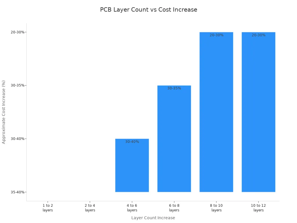
Note: More layers mean more steps, higher skill, and greater cost in pcb manufacturing.
Lamination & Drilling
Lamination Process
You build a strong and reliable PCB by carefully bonding all the layers together. The lamination process joins the copper and insulating layers into one solid board. You must follow each step closely to avoid problems like bubbles, warping, or weak spots.
Here are the key steps in the lamination process:
Preparation: You clean all copper and substrate surfaces to remove dust, oil, and other contaminants. Clean surfaces help the layers stick together and prevent weak spots.
Micro-etching: You roughen the copper surface with a special chemical bath. This creates tiny grooves that help the next layer grip tightly.
Black Oxide Treatment: You apply a black oxide coating to the copper. This coating forms a textured, chemically bonded layer that improves adhesion between copper and the prepreg (the glue-like insulating layer). The oxide coating is especially important for boards with large copper areas, like ground planes, because it helps the board resist heat and stress during use.
Inner Layer Stack-Up: You stack the inner copper layers and prepreg sheets in the correct order. Careful stacking keeps the layers from shifting during lamination.
Full Stack-Up: You add all the layers, including the outer copper sheets, to complete the board’s structure.
Lamination: You place the stack in a heated press. The press uses high temperature and pressure to melt the prepreg and bond all the layers together. You must control the temperature and pressure carefully. Too much heat or pressure can cause bubbles (blistering) or gaps (voids) inside the board.
Hole Registration: You align the drilled holes with the copper pads. Good alignment ensures that the electrical connections work as designed.
Tip: You should always use a cleanroom for lamination. Even tiny dust particles can get trapped between layers and cause short circuits or weak spots. Cleanrooms keep the air free of dust and control temperature and humidity, which helps you make stronger, more reliable boards.
You also need to pay attention to quality control during lamination. You monitor the temperature, pressure, and timing of the press. You check that all layers line up correctly and that there are no air pockets. These steps help you avoid common problems like delamination, warping, or misaligned circuits.
Drilling & Via Formation
After lamination, you drill holes in the board to create paths for electricity to flow between layers. These holes are called vias. You use different drilling methods depending on the size and type of via you need.
Feature | Laser Drilling | Mechanical Drilling | Plasma Etching / FIB Drilling |
|---|---|---|---|
Via Types Supported | Microvia, Blind, Via-in-Pad (VIP) | Through-hole, Blind | Microvia (mainly flex/R&D) |
Minimum Via Size | ~150 µm | <20 µm (FIB) | |
Speed | High | Medium to High | Low |
Equipment Cost | High | Low | High (FIB), Medium (Plasma) |
Material Compatibility | Selective | Broad | Depends on method |
Typical Use Case | HDI, mobile devices | Standard multilayer PCBs | Flexible PCBs, prototyping, research |
You use mechanical drilling for larger holes (above 150 micrometers). This method works well for standard boards but cannot make very small or blind vias. For high-density boards, you use laser drilling. Laser drilling creates tiny microvias (as small as 20 micrometers) with high precision. This is important for smartphones and other compact devices. Plasma etching and focused ion beam (FIB) drilling are special methods used mostly for flexible boards or research.
Note: You must keep your drill bits sharp and use the right speed and pressure. Dull bits or wrong settings can cause rough holes, burrs, or even cracks in the board. Regular maintenance and careful setup help you avoid these problems.
You also need to check the alignment of the holes with the copper pads. Misaligned holes can break the electrical connection and cause the board to fail. Automated machines and optical inspection tools help you keep everything lined up.
Plating & Copper Deposition
Once you finish drilling, you need to make the holes conductive. You do this by adding a thin layer of copper inside each hole. This step is called plating.
Electroless copper plating comes first. You dip the board in a special chemical bath that deposits a thin layer of copper on the walls of the holes. This layer is very thin but covers all surfaces, even non-metallic ones.
Electrolytic copper plating follows. You use an electric current to add more copper, making the layer thicker and stronger. This step ensures that the holes can carry enough current without overheating.
These plating steps give your board high electrical conductivity and strong connections between layers. Uniform copper plating is critical for the board’s performance and reliability.
Quality control is essential during plating. You monitor the thickness and uniformity of the copper layer. You also check for voids or gaps, which can cause open circuits or weak spots. Careful control at this stage helps you achieve high yield rates—modern pcb manufacturing facilities often reach over 99% first-pass yield.
By following these steps and using the right technologies, you create a PCB that is strong, reliable, and ready for the next stages of manufacturing.
PCB Manufacturing Finishing
Solder Mask
You protect your PCB’s copper traces with a solder mask. This layer covers the board and leaves only the pads exposed for soldering. Solder mask prevents short circuits, corrosion, and accidental solder bridges during assembly. You can choose from several types of solder masks, each with its own benefits:
Solder Mask Type | Advantages |
|---|---|
Liquid Photoimageable Solder Mask (LPSM) | High resolution, excellent adhesion, good insulation, many colors, cost-effective for large runs |
Dry Film Photoimageable Solder Mask (DFSM) | Fast application, consistent thickness, best for high-density boards, less setup needed |
Liquid Screen Printed Solder Mask (LSPSM) | Lower cost, quick for prototypes, many color options |
Peelable Solder Mask (PSM) | Protects certain areas, easy to remove, great for rework or repair, low cost |
Most boards use a green solder mask, but you can pick other colors for special needs. Liquid epoxy solder mask is the most common and affordable. If you need high precision and durability, liquid photoimageable solder mask works best. This type uses light to create sharp, reliable openings for pads and vias.
Tip: A good solder mask improves your board’s reliability and makes assembly easier.
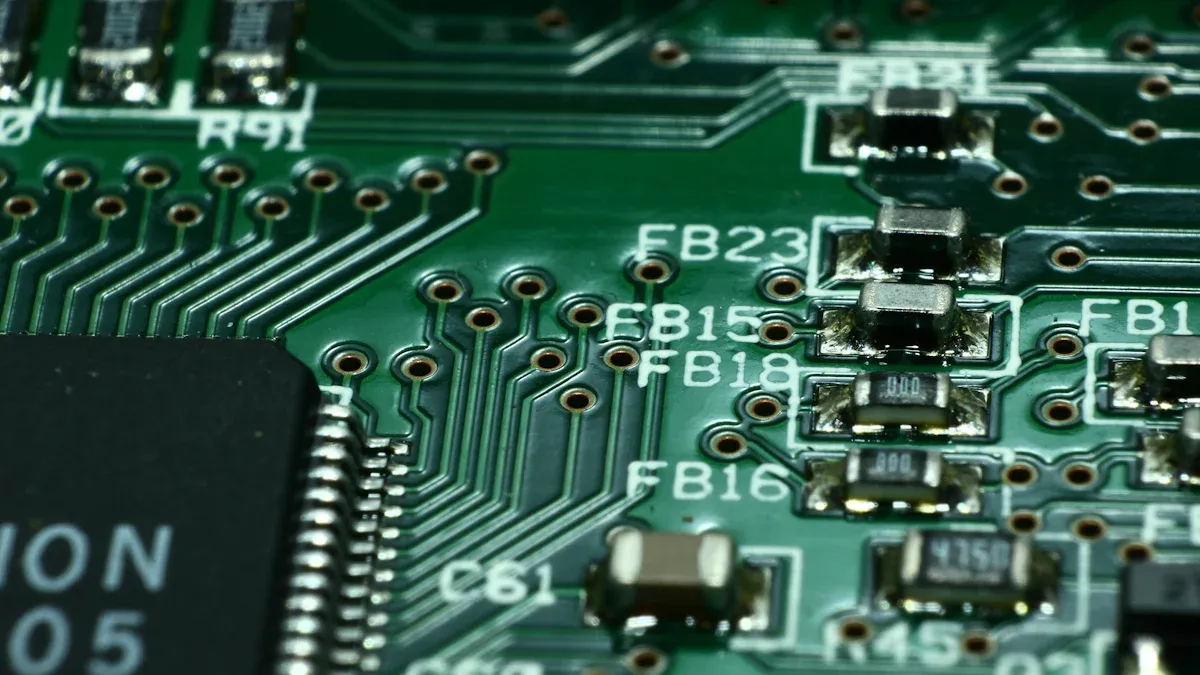
Silkscreen
You add a silkscreen layer to print important information on your PCB. This layer uses ink to show part numbers, symbols, and company logos. Silkscreen markings help you and your team place components in the right spots. You see labels like “R1” for resistors or “C1” for capacitors. Orientation marks show how to install parts correctly.
You can spot missing or misaligned parts during inspection.
Technicians use silkscreen to find and fix problems faster.
High-contrast inks keep markings clear for the board’s entire life.
When you use silkscreen, you make assembly, troubleshooting, and quality control much easier.
Surface Finish
You apply a surface finish to protect exposed copper pads and improve solderability. The finish keeps copper from oxidizing and ensures strong solder joints. Here are the most common finishes and how they affect your board:
Surface Finish | Description & Usage | Impact on Solderability & Assembly |
|---|---|---|
HASL (Hot Air Solder Leveling) | Molten solder coating, leveled with hot air. | Good solderability, uneven surface, low cost, not ideal for tiny parts. |
Lead-Free HASL | Like HASL but uses lead-free solder. | Good solderability, eco-friendly, not flat enough for fine-pitch parts. |
ENIG (Electroless Nickel Immersion Gold) | Nickel and gold layers for flat, corrosion-resistant surface. | Excellent solderability, flat, best for small parts and repeated soldering. |
OSP (Organic Solderability Preservative) | Thin organic layer protects copper. | Flat surface, short shelf life, sensitive to handling, good for fine-pitch and SMT. |
Immersion Silver | Silver layer on copper. | Good solderability, flat, can tarnish, needs careful storage. |
Immersion Tin | Tin layer applied chemically. | Smooth, good for small parts, sensitive to oxidation, short shelf life. |
Gold Plating (Hard/Soft Gold) | Used for connectors needing durability. | Very durable, excellent for connectors, more expensive. |
You should match the surface finish to your assembly process and product needs. ENIG works well for fine-pitch and high-reliability boards. HASL is a good choice for simple, low-cost projects. OSP and immersion finishes suit modern, high-density designs.
Note: The right surface finish helps you get strong solder joints and a reliable product in pcb manufacturing.
Assembly & Testing
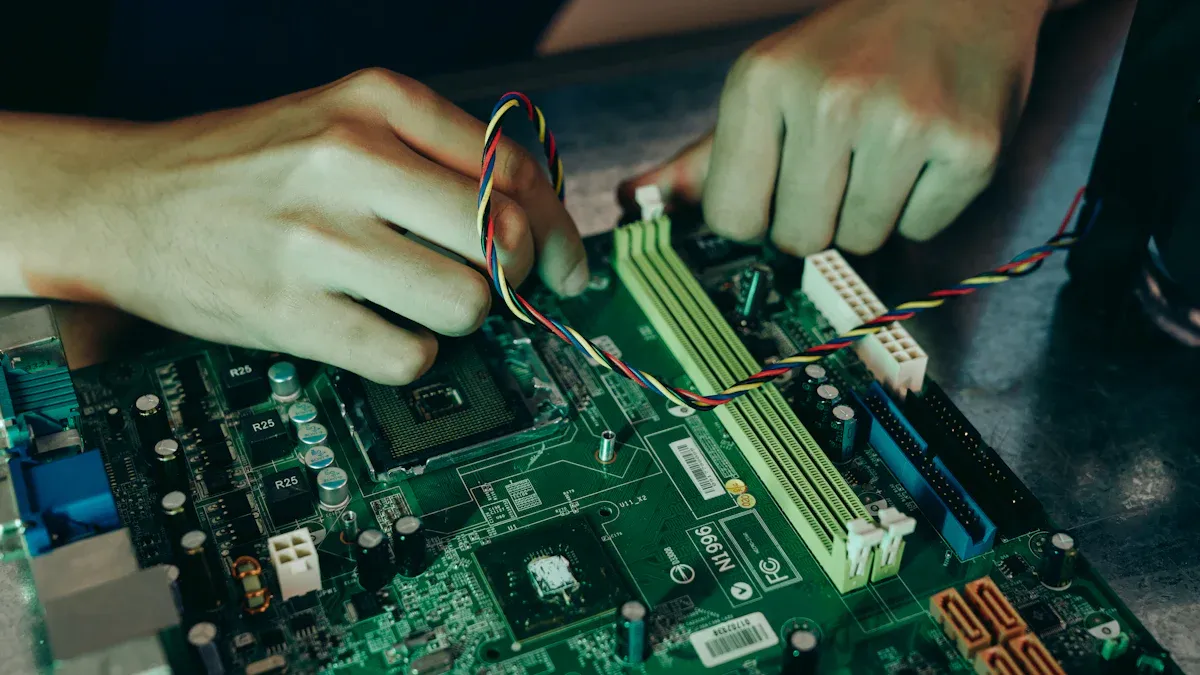
Component Mounting
You bring your board to life by mounting components onto it. You can use different methods, each with its own level of automation and speed. Through-hole technology (THT) lets you insert parts into drilled holes, often by hand. Surface-mount technology (SMT) uses machines to place tiny parts directly onto the board’s surface. Some boards use both methods, called mixed assembly. The table below shows how these methods compare:
Method | Component Placement | Soldering Technique | Automation Level and Speed |
|---|---|---|---|
Through-Hole (THT) | Manually inserted into holes | Manual or wave soldering | Mostly manual; slower; good for strong parts |
Surface-Mount (SMT) | Machines place on solder paste | Reflow soldering in oven | Highly automated; very fast; best for dense, high-volume boards |
Mixed Assembly | Uses both THT and SMT | Both wave and reflow soldering | Complex; needs careful control |
SMT is the most common in modern pcb manufacturing. It gives you fast, accurate, and high-density assembly. THT works best when you need strong mechanical support, such as for connectors or large parts.
Electrical Testing
You must test your board to make sure it works and lasts. You use several types of electrical tests:
Continuity testing checks if current flows where it should.
In-circuit testing (ICT) looks at each part to find mistakes or defects.
Functional testing simulates real use to see if the board meets design goals.
Burn-in testing runs the board at high temperatures to catch early failures.
Capacitance and resistance tests help you find shorts, opens, or missing traces.
Flying probe and fixture testing let you check many points quickly, even in small batches.
Stress testing exposes your board to heat, vibration, and moisture to check durability.
You also use lifecycle tests, like accelerated life testing, to predict how long your board will last. These steps help you deliver reliable products, especially for devices that face tough conditions.
Tip: Careful testing at this stage prevents costly failures later.
Packaging & Delivery
You protect your finished board during shipping by using special packaging methods. Start by cleaning the board to remove dust. Wrap it in an antistatic bag to guard against static electricity. Add bubble wrap or foam inserts for shock protection. Seal the board in a moisture barrier bag to keep out water. Place everything in a sturdy box and fill empty spaces with packing peanuts or foam. Label the box with instructions like “Fragile” and “Handle with Care.”
Use anti-static packaging, such as ESD bags or anti-static bubble wrap, to prevent static damage.
Moisture-proof packaging, like sealed bags with desiccants, keeps your board safe from corrosion.
Cushioning materials, such as foam or bubble wrap, absorb shocks and prevent breakage.
These steps ensure your board arrives safely and ready for use.
When you understand each step in making a printed circuit board, you make better design choices and avoid common mistakes. Careful planning helps you select the right materials, place components for reliability, and use proper testing to catch defects early.
Early reviews and design checks prevent costly errors.
Quality control steps, like visual inspection and electrical testing, improve durability.
Working closely with manufacturers helps you solve challenges and meet high standards.
Paying attention to every detail leads to safer, longer-lasting products.
FAQ
What is the most common material for PCBs?
You usually see FR-4 as the main material. FR-4 gives your board strength and good insulation. It works well for most electronics. You can also find boards made from polyimide, PTFE, or metal for special uses.
How do you check if your PCB design is ready for manufacturing?
You should run a Design Rule Check (DRC) in your PCB software. This tool finds errors like short traces or wrong hole sizes. Always review your Gerber files and BOM before sending them to your manufacturer.
Why do you need a solder mask on your PCB?
A solder mask protects your copper traces from short circuits and corrosion. It also helps you avoid solder bridges during assembly. You get a cleaner, more reliable board with a good solder mask.
What is the difference between SMT and THT assembly?
SMT places parts directly on the board’s surface using machines. THT puts parts through holes, often by hand. SMT works best for small, dense boards. THT gives strong support for large or heavy parts.
How do you make sure your PCB arrives safely?
You should use anti-static bags, bubble wrap, and moisture-proof packaging. These steps protect your board from static, shocks, and water. Always label your package as “Fragile” for extra care during shipping.
See Also
Key Distinctions Between Evaluation And Development Boards
A Comparison Of FPGA Boards From Leading Brands
Analog Devices’ Approach To Maintaining Strong Chip Supply
A Comprehensive Guide To Digital Integrated Electronic Circuits
Essential MOSFET Fundamentals Every Electronics Fan Should Know