Effective Ways to Minimize Noise in Digital ICs
Minimizing noise in digital ICs is essential for ensuring reliable performance. Noise can disrupt signal integrity, leading to errors in data transmission or even system failure. In high-speed, high-density circuits, the challenges become more pronounced. For instance, microvias, with diameters as small as 0.15 mm, are used to reduce parasitics and improve signal quality. They achieve nearly ten times lower parasitics compared to traditional vias. Controlled depth drilling further eliminates unused via barrel sections, enhancing performance. By prioritizing IC noise reduction during design, you can mitigate these risks and build robust circuits.
Key Takeaways
Knowing where noise comes from is important. Find common sources like heat noise and ground bounce early to reduce them.
Use good grounding and shielding methods. These help signals stay clear and lower noise problems in circuits.
Add decoupling capacitors correctly. Put them near IC power pins to keep voltage steady and block high-frequency noise.
Design your PCB layout carefully. A good layout stops signal mixing and reduces electromagnetic interference, making circuits work better.
Focus on managing clock and signal timing. Methods like Clock Tree Synthesis keep signals in sync and lower timing mistakes.
Understanding Noise in Digital ICs
Common Sources of Noise
Noise in digital ICs originates from various sources, each contributing to signal degradation. One common source is 1/f noise, which occurs due to imperfections in semiconductor materials. Another is thermal noise, also known as Johnson noise, caused by the random movement of electrical charges in resistors. This type of noise depends on temperature and bandwidth, making it a fundamental concept in circuit analysis. Additionally, simultaneous switching of outputs in ICs generates ground bounce, a significant noise source in high-speed circuits.
Other contributors include power supply fluctuations and electromagnetic interference (EMI) from nearby components. As IC technology advances, the integration of multiple functionalities on a single chip increases the complexity of noise management. You must identify these sources early to implement effective IC noise reduction strategies.
Types of Noise: Crosstalk, Ground Bounce, and Power Supply Noise
Crosstalk, ground bounce, and power supply noise are distinct but often interrelated. Crosstalk arises from inductive or capacitive coupling between signal traces, leading to unwanted voltage spikes. Ground bounce, on the other hand, occurs when the ground plane potential fluctuates due to simultaneous switching of outputs. This phenomenon can disrupt signal integrity, especially in circuits with high pin counts.
Power supply noise stems from variations in the voltage supply (Vcc). As supply voltages decrease in modern ICs, noise margins shrink, making circuits more sensitive to even minor fluctuations. This sensitivity can result in clock jitter and degraded transceiver performance. Understanding these noise types helps you diagnose and address signal integrity issues effectively.
Effects of Noise on Circuit Performance
Noise significantly impacts circuit performance. For example, studies show that noise can increase the Bit Error Rate (BER) in communication systems. In one scenario, injecting a 1 MHz continuous wave (CW) tone into a noisy channel degraded the BER from 1E-07 to 7E-05. This demonstrates how noise can compromise data accuracy.
High noise levels also lead to timing errors, causing clock signals to misalign. This misalignment disrupts data synchronization, affecting overall system reliability. By prioritizing IC noise reduction during design, you can minimize these risks and ensure optimal circuit performance.
IC Noise Reduction Techniques
Proper Grounding and Shielding
Proper grounding and shielding play a vital role in minimizing noise in digital circuits. Grounding cable shields at one end is a common practice to prevent ground loops. However, for longer distances, grounding at both ends may be necessary to stop noise currents from flowing through the shield. Magnetic field noise can induce voltages in circuits, which are difficult to shield against. You can reduce this interference by minimizing the strength of the magnetic field and optimizing the geometry of wiring.
To further reduce induced voltage from magnetic coupling, shorten conductors or decrease their distance to minimize the area of the receiver loop. These adjustments help lower the impact of magnetic noise on your circuit. By implementing proper grounding and shielding techniques, you can significantly improve signal integrity and reduce the risk of noise-related issues.
Effective Use of Decoupling Capacitors
Decoupling capacitors are essential for stabilizing power delivery networks (PDNs) and reducing noise. These capacitors act as local energy reservoirs, supplying current to ICs during transient events and filtering out high-frequency noise. When placed close to the power pins of ICs, they help maintain a stable voltage supply, ensuring reliable circuit operation.
Research highlights the importance of evaluating the long-term reliability of PDNs. Aging and temperature effects can degrade the performance of decoupling capacitors over time, impacting overall PDN functionality. By considering these factors during design, you can mitigate excessive performance degradation and ensure consistent noise reduction.
To maximize their effectiveness, use a combination of capacitors with different values. Smaller capacitors filter high-frequency noise, while larger ones handle low-frequency fluctuations. This layered approach ensures comprehensive noise suppression across a wide frequency range.
Supply Current Shaping
Supply current shaping is another effective method for IC noise reduction. By controlling the current drawn by ICs, you can minimize fluctuations in the power supply and reduce noise. Techniques like slew rate control limit the rate at which current changes, preventing sudden spikes that could disrupt signal integrity.
Advanced methods, such as non-harmonic analysis (NHA), have proven effective in extracting signals from noisy environments. Studies show that NHA achieves approximately a 2 dB improvement in signal-to-noise ratio (SNR) compared to traditional discrete Fourier transform (DFT) methods. This improvement highlights the potential of supply current shaping techniques in enhancing circuit performance.
When designing circuits, consider implementing current shaping strategies to reduce noise and improve overall system reliability. These techniques not only enhance signal integrity but also contribute to the long-term stability of your design.
Passive Low-Pass Filtering
Passive low-pass filters are effective tools for reducing high-frequency noise in digital ICs. These filters allow low-frequency signals to pass while attenuating unwanted high-frequency components. You can use them to improve signal integrity and reduce interference in your circuits.
Key metrics validate the effectiveness of passive low-pass filtering:
Insertion loss measures the signal loss as it passes through the filter, ensuring minimal impact on desired signals.
Cut-off frequency defines the point where the filter begins to suppress high-frequency noise, providing a benchmark for performance.
Attenuation characteristics describe how well the filter reduces unwanted noise, ensuring reliable circuit operation.
When designing circuits, select filters with appropriate cut-off frequencies based on your application's requirements. For example, a filter with a lower cut-off frequency is ideal for suppressing high-frequency noise in sensitive analog circuits. By incorporating passive low-pass filters, you can achieve significant IC noise reduction and enhance overall system reliability.
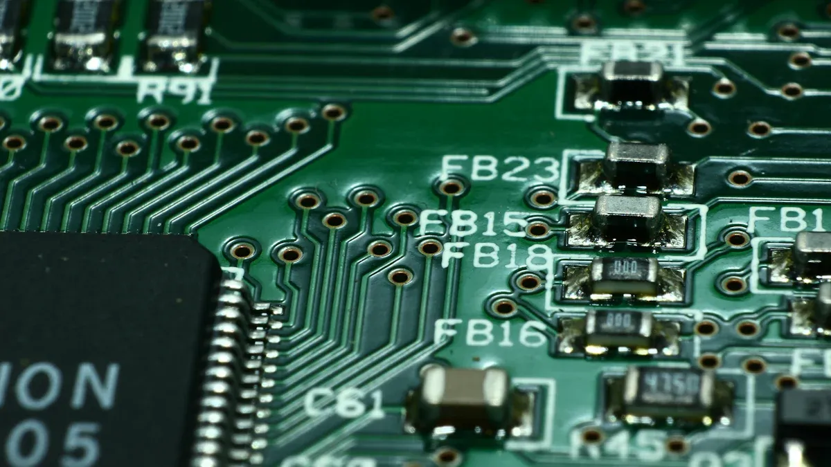
Optimizing PCB Layout and Signal Traces
Optimizing your PCB layout is crucial for minimizing noise and ensuring signal integrity. A well-designed layout reduces crosstalk, ground bounce, and electromagnetic interference, which are common sources of noise in digital ICs.
Here are some guidelines for effective PCB layout optimization:
Guideline | Description |
|---|---|
Recognize sensitive current paths and place components to avoid noise issues. | |
PCB Floor Plan | Minimize current loop areas and arrange power components for smooth current flow. |
Component Placement | Position power components close together to reduce inductance and improve decoupling. |
Additional tips include:
Use ground and power planes extensively to provide stable reference points for signals.
Keep signal traces short and thin, ideally less than 8 mm thick and 4 to 8 mil wide.
Maintain a distance between adjacent traces greater than their width to reduce crosstalk.
Multilayer PCBs are highly recommended for separating ground, power, and signal layers. This separation ensures a clear return path for high-frequency signals, reducing noise and improving circuit performance. By following these guidelines, you can optimize your PCB layout for effective IC noise reduction.
Clock and Signal Integrity Management
Maintaining clock and signal integrity is essential for ensuring synchronized operations in digital circuits. Noise can cause clock skew and jitter, leading to timing errors and degraded performance. You can address these issues by implementing strategies like Clock Tree Synthesis (CTS).
CTS distributes the clock signal efficiently across the circuit, minimizing skew and jitter. This ensures that all components receive the clock signal simultaneously, maintaining synchronization. Physical verification processes also play a critical role in preserving signal integrity. These processes confirm that the chip layout meets specifications, addressing issues related to power distribution and signal routing.
To further enhance signal integrity, use differential signaling for high-speed data transmission. Differential pairs reduce susceptibility to noise by transmitting signals as voltage differences rather than absolute values. Additionally, shield critical signal traces to prevent electromagnetic interference.
By prioritizing clock and signal integrity management, you can achieve reliable circuit performance and reduce the impact of noise on your design.
Analyzing and Measuring Noise
Tools for Noise Measurement
To measure noise in digital ICs effectively, you need the right tools and methodologies. These tools help you analyze noise behavior and identify its impact on circuit performance. Below is a table summarizing common noise measurement modes and their applications:
Mode | Description |
|---|---|
Timeaverage | Calculates noise power averaged over all PSS timepoints, ideal for noise figure and oscillator phase noise measurements. |
Sampled | Measures noise at specific time points in PSS analysis, useful for outputs crossing a threshold. |
Edge Crossing | Measures noise on a net defined by an edge, allowing for multiple threshold measurements. |
Edge Delay | Measures noise defined by two edges, useful for pulse noise measurements and jitter calculations. |
Sampled Phase | Measures noise at different points in an edge, though it lacks direct plot functions for jitter calculation. |
These tools allow you to pinpoint noise issues and evaluate their effects on your circuit. By selecting the appropriate mode, you can gain deeper insights into noise behavior and improve your design.
Identifying Noise Sources
Identifying noise sources is a critical step in noise management. Noise can originate from various components and environmental factors. Here are some real-world examples and common causes of noise in digital circuits:
An investigation revealed that a disconnected ground conductor in a wiring box caused high levels of ground noise.
Shared power sources between systems led to interference, highlighting the importance of isolating power supplies.
Installing a ground noise filter reduced noise affecting electronic HID lights, improving performance.
Additionally, digital circuits themselves can act as noise sources. Rapid signal transitions between 0 and 1 generate a wide range of frequency components. To mitigate this, you should use shields and EMI suppression filters. Digital signals are also vulnerable to pulse noise, such as electrostatic discharge (ESD), which can disrupt circuit functionality. By addressing these sources, you can minimize noise and enhance circuit reliability.
Quantifying Noise Levels
Quantifying noise levels helps you understand its impact on your circuit. Engineers use several measurement standards and statistical techniques to evaluate noise. The table below outlines some common methods:
Measurement Standard/Technique | Description |
|---|---|
Noise Figure | Measures the degradation of the signal-to-noise ratio (SNR) as it passes through a circuit. |
Noise Factor | Represents the ratio of input SNR to output SNR, always greater than one. |
Noise Temperature | Expresses noise power in a circuit, measured in Kelvin. |
Y-factor Method | Compares output noise at two different temperatures to calculate the noise figure. |
These techniques provide a clear picture of noise performance in your design. For instance, the noise figure helps you assess how much noise your circuit adds to the signal. By applying these methods, you can ensure your circuit meets performance requirements and operates reliably.
Implementing and Validating Noise Reduction
Applying Mitigation Techniques in Design
Applying noise mitigation techniques during the design phase ensures that your circuit performs reliably under real-world conditions. By addressing noise sources early, you can prevent costly redesigns and performance issues. Several proven strategies can help you achieve this goal.
For instance, using PMOS transistors in the input stage of differential amplifiers eliminates 1/f noise, which is common in semiconductor materials. A good differential layout, combined with guard rings and triple-well isolation, minimizes noise coupling through the supply or substrate. Additionally, implementing P+ guard rings around sensitive analog circuits protects them from high-frequency noise. Studies show that P+ guard rings are particularly effective in suppressing such interference.
The table below summarizes these techniques and their practical applications:
Technique Description | Application |
|---|---|
Use of PMOS transistors for input in differential amplifiers | Eliminates 1/f noise |
Good differential layout with guard rings and triple well isolation | Reduces noise coupling via supply or substrate |
P+ guard ring implementation | Protects analog circuits from high-frequency noise |
Majority of work indicates P+ guard ring is effective | Suppresses high-frequency noise |
By incorporating these techniques into your design, you can significantly enhance IC noise reduction and improve overall circuit performance.
Tip: Always simulate your design under various noise conditions to validate the effectiveness of these techniques before moving to the prototyping stage.
Testing and Validating Noise Reduction
Testing and validation are critical steps in ensuring that your noise reduction strategies work as intended. You can use specialized tools and methodologies to measure noise levels and assess their impact on circuit performance.
Start by conducting noise measurements under different operating conditions. Use tools like spectrum analyzers and oscilloscopes to capture noise behavior. Focus on key parameters such as signal-to-noise ratio (SNR), noise figure, and jitter. These metrics provide valuable insights into how well your design suppresses noise.
Validation also involves stress testing your circuit. For example, you can introduce controlled noise sources, such as electromagnetic interference (EMI), to evaluate your circuit's resilience. This approach helps you identify weak points and refine your design further.
Note: Testing should include both static and dynamic conditions. Static tests measure noise levels in a steady state, while dynamic tests assess performance during transient events like switching or power fluctuations.
By thoroughly testing and validating your design, you can ensure that your noise reduction strategies meet the required performance standards.
Iterative Design Improvements
Noise reduction is not a one-time effort. Iterative design improvements allow you to refine your circuit over multiple cycles, addressing new challenges as they arise. This approach ensures that your design remains robust and adaptable to changing requirements.
One documented method for iterative improvement is Cycle Benchmarking (CB). This protocol estimates the fidelity of noise processes in quantum devices. It is robust against state preparation and measurement (SPAM) errors and requires minimal measurements, regardless of the system's complexity. Another technique involves process fidelity estimation, which evaluates the quality of a noisy process by comparing it to an ideal target. Engineers often use Pauli matrices for this purpose.
The table below highlights these iterative methods:
Evidence Description | Key Points |
|---|---|
Cycle Benchmarking (CB) | Estimates process fidelity of noise processes; robust to SPAM errors. |
Process Fidelity Estimation | Evaluates noisy processes using Pauli matrices; sensitive to SPAM errors. |
Random Pauli Cycle (R) | Introduces random Pauli cycles to engineer noise as a Pauli noise channel. |
By adopting these iterative techniques, you can progressively enhance your design's noise resilience. Each cycle provides an opportunity to identify weaknesses, implement improvements, and validate their effectiveness.
Tip: Document each iteration thoroughly. This practice helps you track progress and ensures that future designs benefit from past learnings.
Minimizing noise in digital ICs is essential for maintaining reliable performance and signal integrity. Noise disrupts circuits, causing timing errors and data inaccuracies. By understanding its sources and effects, you can implement effective strategies to reduce interference and improve system reliability.
Key Techniques and Applications
Early analog noise reduction schemes improved listening ease.
Digital Noise Reduction (DNR) enhances speech recognition in noisy environments like cars and traffic.
Outcomes of DNR systems vary across manufacturers, emphasizing the importance of tailored solutions.
Technique | Application Description |
|---|---|
Differential Signaling | Cancels out common-mode noise in data transmission standards like USB and HDMI. |
Ferrite Beads | Blocks high-frequency noise in power supplies and signal paths. |
Low-Pass Filters | Allows low frequencies to pass while blocking high-frequency noise in audio systems. |
Spread Spectrum Clocking | Reduces noise energy in RF and communication systems by spreading clock signal frequency. |
Capacitive Coupling | Isolates noise sources in signal lines and amplifier circuits. |
Signal Termination | Prevents signal reflections in high-speed interfaces. |
Power Supply Noise Isolation | Isolates noisy and quiet power supplies in mixed-signal circuits. |
Tip: Proactively address noise during design and testing phases. Iterative improvements ensure your circuit adapts to new challenges and maintains optimal performance.
By applying these techniques and continuously refining your design, you can build robust circuits that perform reliably in real-world conditions.
FAQ
What is the most common source of noise in digital ICs?
Thermal noise, caused by the random movement of electrical charges, is the most common source. It depends on temperature and bandwidth. You can reduce its impact by using proper grounding, shielding, and decoupling capacitors.
How do decoupling capacitors help reduce noise?
Decoupling capacitors stabilize power delivery by acting as local energy reservoirs. They filter high-frequency noise and maintain a stable voltage supply. Place them close to IC power pins for maximum effectiveness.
Why is PCB layout important for noise reduction?
A well-designed PCB layout minimizes crosstalk, ground bounce, and electromagnetic interference. Short signal traces, proper spacing, and multilayer PCBs improve signal integrity and reduce noise.
Can passive low-pass filters eliminate all noise?
Passive low-pass filters effectively reduce high-frequency noise but cannot eliminate all noise. Use them with other techniques like shielding and decoupling capacitors for comprehensive noise management.
What tools can you use to measure noise in circuits?
You can use spectrum analyzers, oscilloscopes, and noise figure meters. These tools help you analyze noise behavior, identify sources, and evaluate the effectiveness of your noise reduction strategies.
Tip: Regularly test your circuit under different conditions to ensure reliable performance.
See Also
Proven Methods to Address Electronic Component Supply Issues
Emerging Developments Influencing the Analog IC Sector by 2025
Exploring Low Power IoT Chip Tech and Its Uses